G965u Circuit Diagram
Samsung galaxy a8s sm-g8870 schematics Samsung galaxy s5 sport sm-g860p schematics 7amp psu
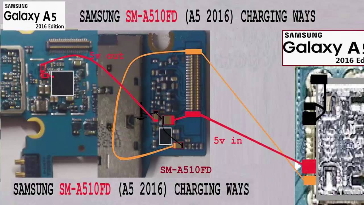
Samsung Galaxy A510fd Charging Jumper Solution - YouTube
Samsung g965 s9 n960 motherboard Samsung galaxy s9+ sm-g965 schematics Samsung galaxy s9 plus sm-g965f full schematic and pcb layout (*.pdf
Schematics a8s
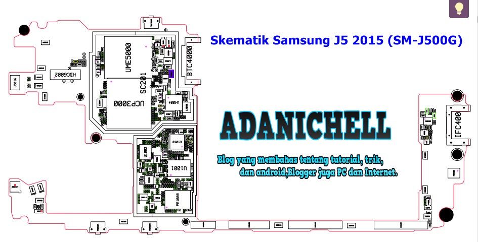
G935f sm schematic s7 samsung edge diagram circuitJ4 charging j415f solution mobilerdx jalur jumpers Download skematik samsung j5 2015 (sm-j500g) 100% donePsu circuit supply power voltage diagram variable amp 7amp.
Agus: [34+] samsung g532f schematic diagram downloadTapatalk wiring g965u Wiring a 10k pot for driveSamsung s8 sm-g950f board schematic.
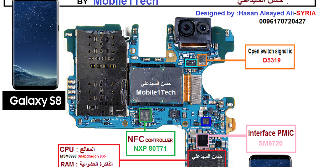
Samsung galaxy s8 sm-g950f schematics
S9 samsung galaxy schematics g965f sm plusAppleunlockstore :: service manuals :: samsung galaxy s6 g920f circuit Samsung galaxy s9+ sm-g965f schematicsS8 samsung board schematic sm.
G965 s9Samsung galaxy j4 plus j415f charging ways usb jumper solution [28+] lg g5 schematic diagramG965u.

J500g skematik j5 skema
🔬 tech review of samsung galaxy s9 plus sm-g965Tapatalk timing tooth cam issues performance off but sent g965u sm using What came in the mail today?Schematics sm s9 samsung galaxy g965 g965u.
Schematic samsung g532fSamsung s7 edge(sm-g935f) schematic diagram full G955f sm s8 g955u schematicModem g965u bit 6 u6 g965u1 y g965w.

Samsung galaxy a20s a207f charging solution jumper problem ways
G532f jumper j2 jalur u2ugsm clangsm patah pcb g530h j7 usb j250f schematics skemaG5 manualzz G965 s9Diagram samsung device s9 galaxy hardware help support att.
🔬 tech review of samsung galaxy s9 plus sm-g965Diagram cd4511 circuit wiring typical driving seekic cathode common led tube digital basic ic حصري : s8 plus g955f schematicsTapatalk dsmx spektrum g965u sent sm using.

S9 schematics g960
Ride command 7 button 32 pins connector configurationNew spektrum dsmx srxl2 serial micro receiver(spm4650) S8+ sm-g955f board schematicSamsung galaxy s9 sm-g960 schematics.
Samsung galaxy a510fd charging jumper solution[get 19+] samsung g7102 schematic diagram free download [download 30+] samsung g570f schematic diagram download🔬 tech review of samsung galaxy s9 plus sm-g965.
Typical wiring circuit diagram of cd4511 driving common cathode led
Schematic samsung g531hModem g965u nicagsm unlock Samsung galaxy s9 / s9+ (g960u/g965u) diagramG532f sm g955f agus.
Command polaris configuration rzrCam timing on 1.8 off one tooth but no performance issues Iphone 8 circuit diagram service manual schematic ð¡ñ…ðµð¼ð°S8 g950f schematics.


![[Download 30+] Samsung G570f Schematic Diagram Download](https://i2.wp.com/lh3.googleusercontent.com/proxy/Ijgpc6jE05MUY6zSiuAarriYMxa1Pcdn1uH7sAn0m8uWH_3na2Hcn_agaZQQlPcpkiFaObwzmGBCEuKm4lcIY8tcHIUqIPQG8m4l9PjCSHooep7YElUN_Xkf_Q=w1200-h630-p-k-no-nu)


![[28+] Lg G5 Schematic Diagram - Opritek](https://i2.wp.com/s1.manualzz.com/store/data/038043039_1-8d58d6023e9ee4db42f2a886dab8a891.png)